Leap Motion Teardown
 SFUptownMaker
Introduction
Here at SparkFun, we love gadgets and gizmos, just like our customers. And, like many of you, we find ourselves frustrated all too often by shallow reviews that focus on the "gee whiz!" factor of fancy new electronics without really taking the time to tear into the nitty gritty of how a device works.

As the release of the Leap Motion draws nearer, we're all wondering, what does it do? Demos and shiny PR video aside, what's actually going on in there? And how?
One of our developers got his hands on one (through completely legitimate means; he registered as a developer and ordered it from the manufacturer), and when Nathan sent out an e-mail lamenting the fact that he didn't have one to tear apart, the reply was quick and awesome.
We shot a little video using the visualizer application that is included in the SDK to connect the reality of my hands with the virtuality of the output of the sensor. Check it out!
Now let's get into the teardown proper...
The Outside
Seamless, glossy, and totally devoid of visible fasteners, the Leap Motion has the brushed-aluminum minimalist design which is the new "bent-sheet-metal-and-beige-plastic" aesthetic. The only notable external features are a tiny diffused plastic LED indicator window and data port on one end.
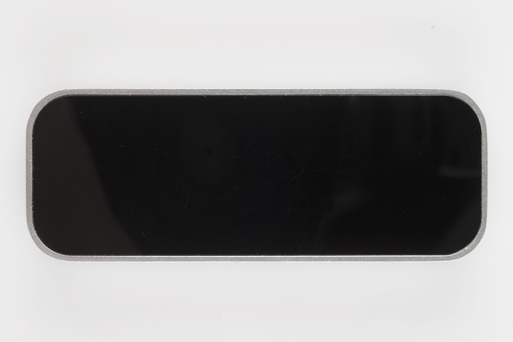
The top surface has the sort of coloration that suggests infrared transparency. It's mildly flexible to the touch, so we know it's plastic. It's also absolutely perfect for attracting and holding smudges, but the software will actually warn you that there's a smudge on the surface, and that's pretty dang cool.

On the underside, there's a subtly embossed rubber sheet, with the typical flim-flam one expects on a consumer product- agency approvals, tiny "recyclable" and "don't trash me" symbols, "Made in China", etc etc. The rubber has a really nice grippy feeling to it- on a whim I put the device on a sheet of acrylic and tipped it up until it started to slide. That was at about 50° above horizontal; if my high school physics lab memories are correct, that's a coefficient of friction of about 1.2. Although it's not very heavy (about 32g, according to our postal scale), the rubber sheet on the bottom keeps in admirably still on my desk.
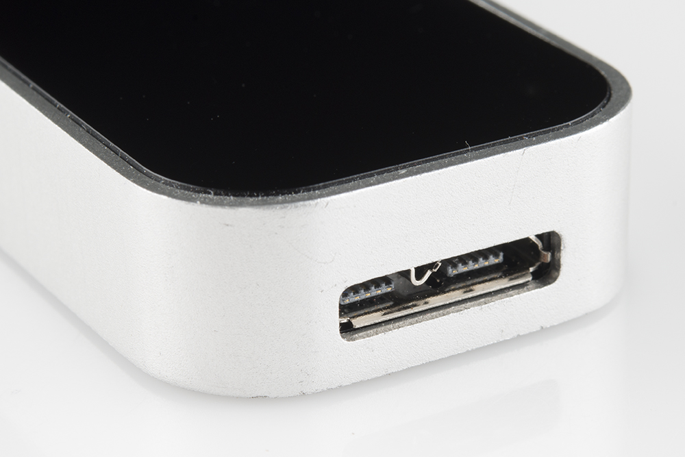
The Leap is tiny- 6.2mm thick, 25mm wide and 75mm long. At one end you'll find the data port- a USB 3.0 micro-B connector. While it can be used as a 3.0 device, I found it worked just fine with a standard USB micro-B connector, plugged into a USB 2.0 port. I'm guessing that chokes your framerate a bit, but I was still seeing framerates up near 200fps, which is pretty darn good.
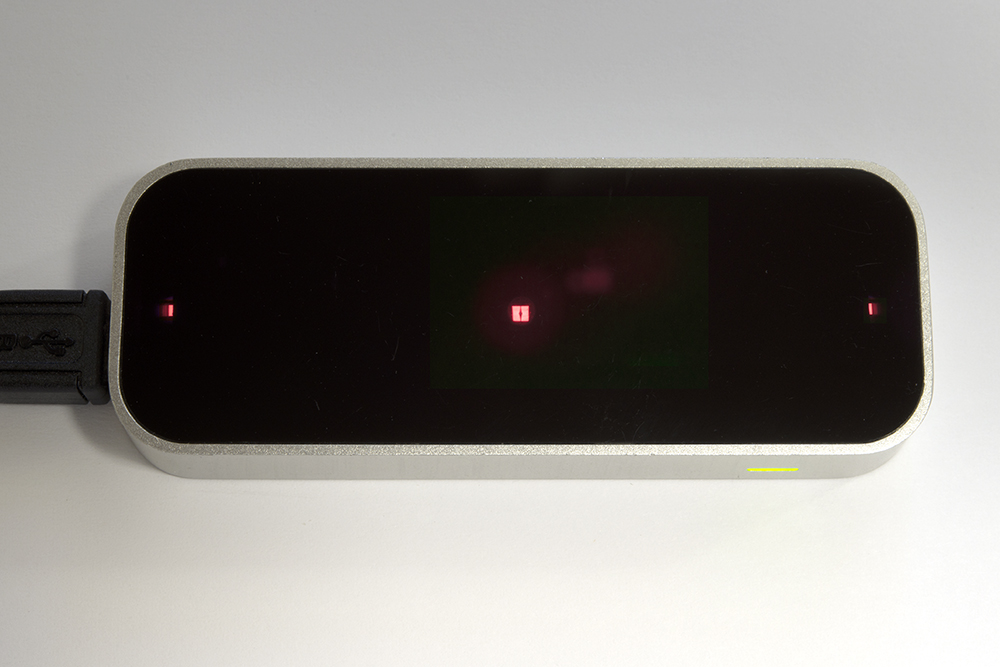
You can see here that there are three infrared LEDs inside, and that they're positioned to provide a nice, wide coverage area. We'll look at those more when we've gotten the cover off. A really cool feature that I noticed as I was playing around with the device is dynamic LED driving- as you move your hand closer to the sensor, the device will automatically dim the LEDs to prevent the imagers from becoming saturated and to keep the data quality high. It's visibly noticeable--the LEDs must be at a very near infrared wavelength (probably near or below 800nm), because they're visible, if barely, to the naked eye.
I stuck a meter in line with the unit to measure the current; once the Leap was in full swing, it was drawing about 320mA. Moving your hand towards it to cause it to dim the LEDs will reduce the current draw to about 200mA. It is warm to the touch, but not unpleasantly so--definitely not warm enough to melt hot glue, so that's an option for securing it to the robot I know you're already thinking of building with it.
Peeling the Onion
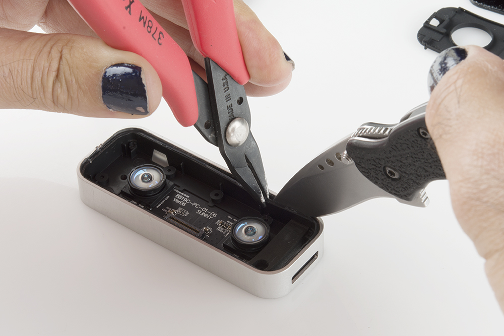
As is so often the case these days, there's no obvious point of entry into the Leap. So, I assumed glue and started a-peelin'.
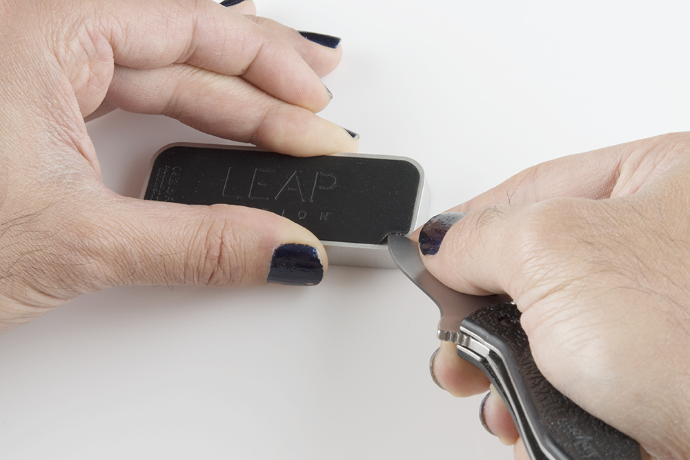
The rubber sheet on the bottom seemed like a great place to start; after all, it's not functional or terribly fragile. Armed with my trusty Kershaw Scallion, I slowly and carefully stripped the rubber sheet off the bottom.
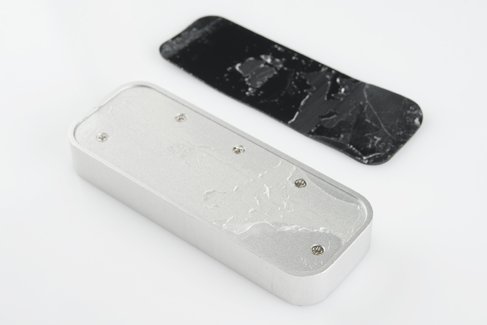
Beneath, I found five tiny screws. Bonus points to the Leap Motion folks for not using tamper-resistant screws- I really appreciate that! A Philips 0 screwdriver took the screws right out, and that didn't do squat as far as improving access to more innards was concerned. We'll see why that is in a bit.
I briefly entertained the fantasy that the guts would pop out if I poked something into the screw hole and pushed; a bit of gentle prodding quickly disabused me of that notion. Without knowing exactly what I was poking I was disinclined to apply any real force...which brought me back to prying.
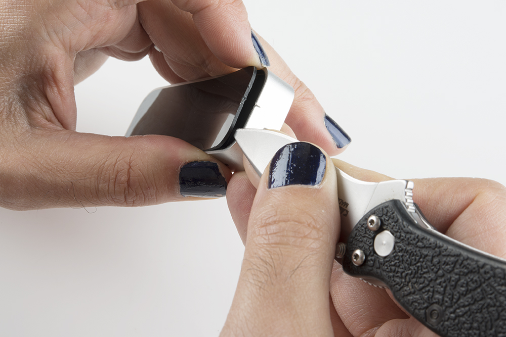
At first, I couldn't get enough of my knife-cum-spudger into the crack between the plastic and the case to make any real headway. I took a fine-tooth saw and cut a tiny notch in the case, and that was just enough to sneak the knife in and release some tension. After that, it was smooth sailing, except when I cracked the plastic a teeny, tiny bit.
You Got Guts, Kid...
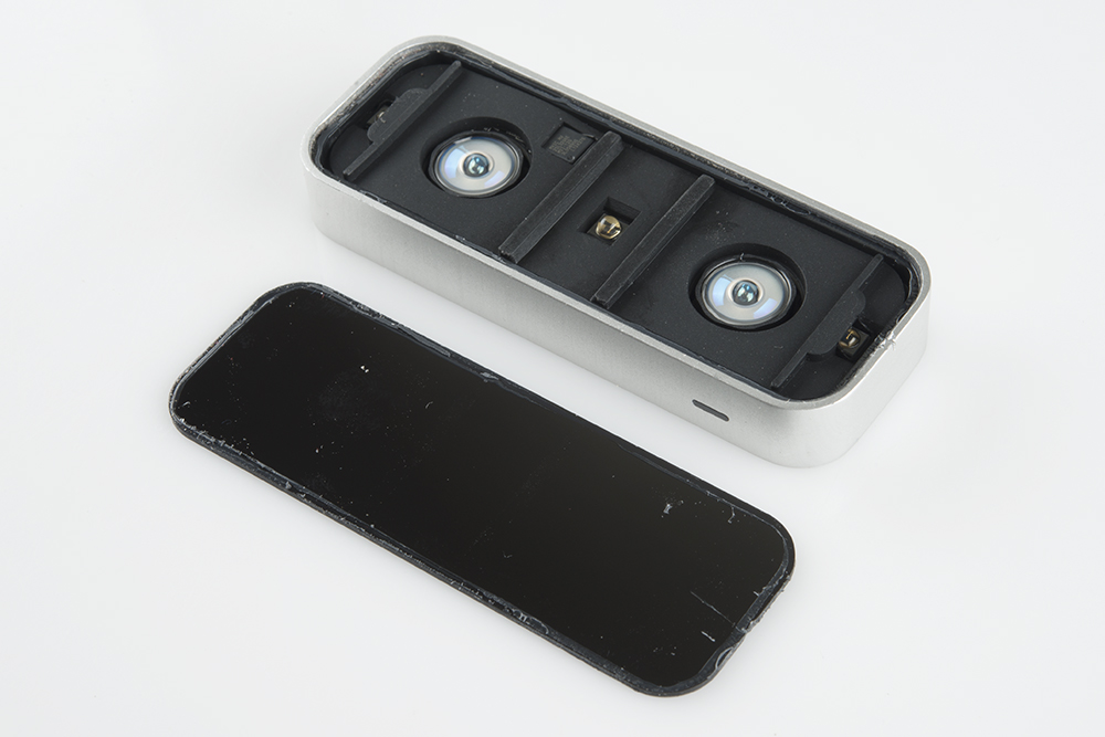
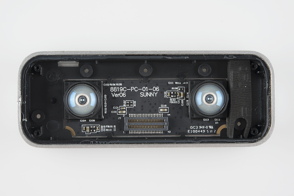
Finally, something interesting! Beneath the plastic is another rubber sheet, with holes for the three LEDs, two sensor elements, and one IC that was apparently a bit too thick to fit otherwise.
In the top-down view, you can see some interesting things. First off, the rubber sheet is clearly design to baffle the light, stopping light bouncing around inside the chassis from reaching the detectors. Secondly, the LEDs on the sides are not only baffled against bleeding over to the detectors, they're also partially shielded to change the area the light is projected into. As nearly as I can tell, there's no synchronization among the LEDs; it would appear that the three LEDs are placed mostly to provide a solid, wide-angle infrared flood of the area of interest, rather than to provide any kind of magical illumination pattern like the Kinect uses. The baffling seems to be in place to prevent a "hotspot" where two LEDs overlap.
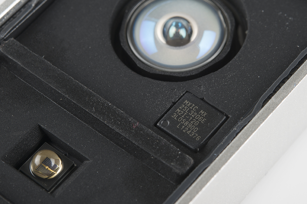
The IC peeking through the rubber isn't anything really exciting--just a 32Mbit serial NOR flash in an 8-pin SOIC package. It's surprising to see it in such a large package, but I'm sure they had good reasons for that. NOR flash is more common in applications like this one, where lots of program erase cycles aren't expected; the write leveling and bad block avoidance which typically accompanies NAND flash would simply add cost.
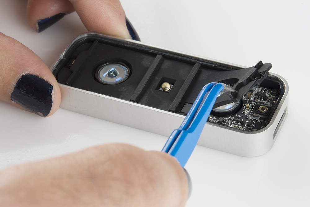
Peeling away the rubber baffle (which is glued, lightly, to the PCB underneath) reveals the top of a two-sided PCB. The top side is mostly bookkeeping: power supplies, the LED drivers, the LEDs themselves. There are three points of interest, however.

In the upper left corner, you can see a three-point serial port- RX, TX and GND. I didn't dig into it too far, but I was able to narrow it down to a 3.3V signal. It didn't dump any data in the first few seconds after power up, so I can't tell you what the data rate is.
In the upper right corner, there's a power supply circuit. This caught my eye because the inductor in the circuit is globbed over with a healthy dose of epoxy, which suggests that at some point in their development cycle, they discovered that it tends to come off the board and took a step to remedy that. Kudos on thorough testing and mitigation!
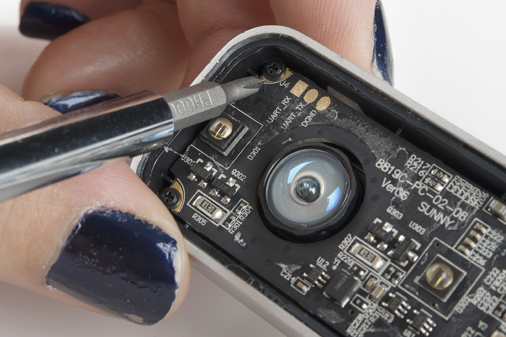
The third point of interest is the bare copper in the corners. I'm a little surprised to see that, as the screws on those points are black oxidized and they screw into a plastic holder, but it wouldn't surprise me if that's a throwback to an earlier version, or a "better-safe-than-sorry" sort of thing.

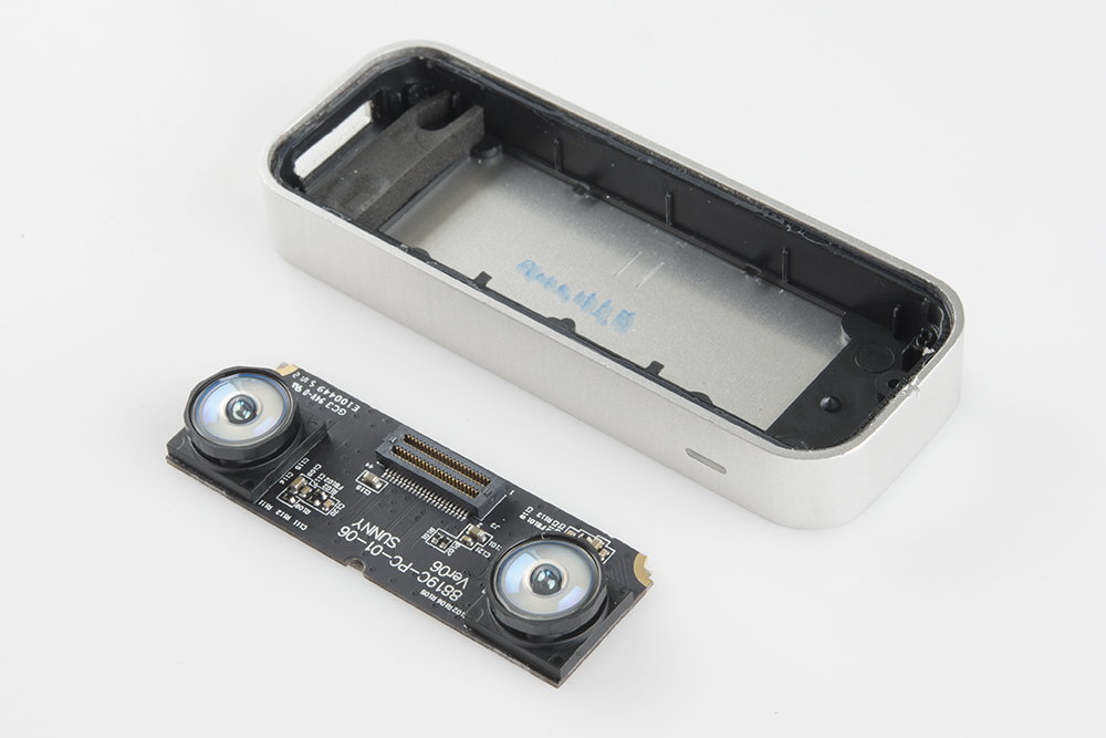
After I removed those screws, the top board lifted out easily, revealing another board and a surprising amount of empty space.

The back side of the top PCB has fewer, but larger, components: two large tantalum capacitors to guard against power supply brown-out during surge currents, a large surface-mount MOSFET (probably part of an inrush current limiting circuit, or supplying power to the LEDs), a fine-pitch dual-row connector to the second PCB, and the brains of the operation.
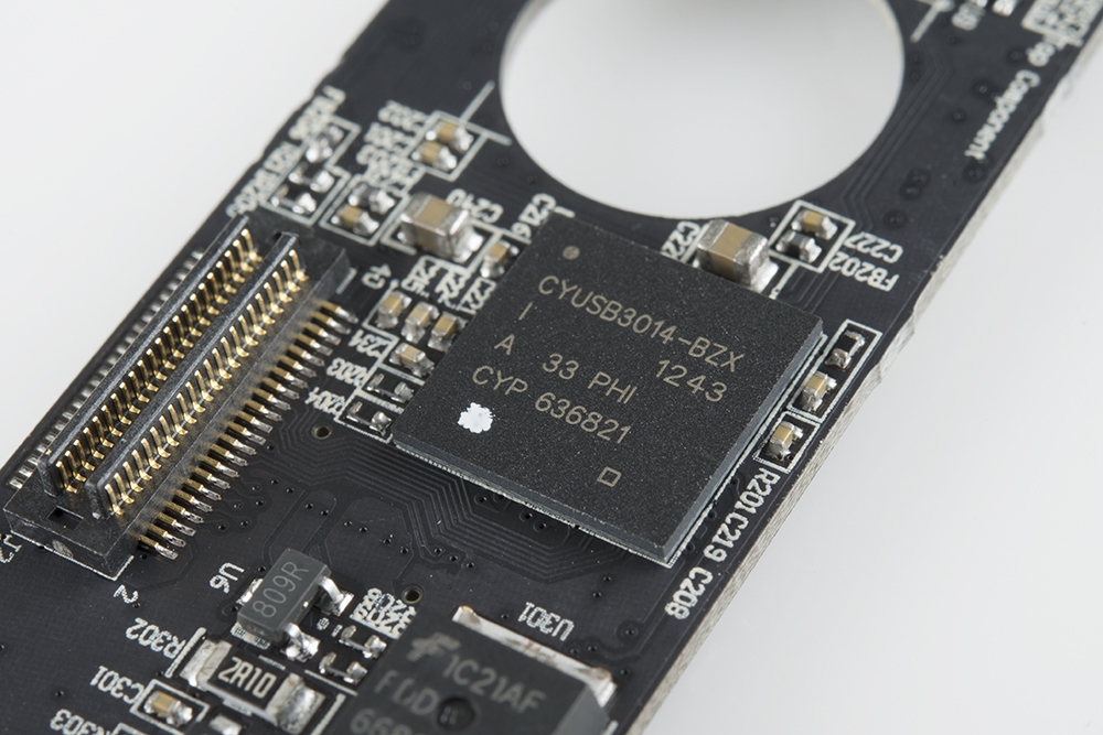
The core functionality of the Leap Motion is provided by a Cypress PSoC part, the CYUSB3014, specifically. If you've never looked into the PSoC parts before, I highly recommend doing so--they're pretty rad. PSoC (for Programmable System on a Chip) are different to standard MCUs because they provide analog and digital blocks which can be reconfigured to suit the user's needs. For instance, one application may need a DMA controller while another needs multiple capture/compare timers, but both can be serviced by the same part simply by altering the firmware to change the disposition of the system's blocks.
Whoops, I flubbed that, big time. The part is actually just a general purpose USB 3.0 device controller with built-in USB 3.0 PHY. The implication there is that all of the work is done on the PC side, and the Leap Motion is just shuffling data from the detectors to the PC as fast as it can manage. That said, I stand by my comments about the PSoC parts above. They are really cool.
Thanks for pointing out my mistake, IRC users Krain and Robint91!
The Seedless Underbelly
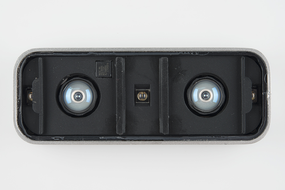
We're down to the end, now--just the one PCB left, nestled down inside a plastic cradle. The lenses over the detectors give the thing an owlish appearance; I didn't try to peel off the optics because I didn't want to permanently damage it, and getting dust between the lens, the aperture and the detector seemed like a bad idea. I also knew that, short of unsoldering the detectors (and even then), I wasn't likely to gain any insight into them other than what I can tell from this view: they're CMOS, not CCD, and that's hardly surprising. The all-in-one functionality of CMOS imagers versus the complexity of CCD imagers support circuitry means that a CCD-based solution would be almost impossible to fit into this footprint.
As to why there are two detectors, it would appear that stereoscopic imaging is very important to this application. Cover up one of the sensors but not the other and the Leap completely fails.
I gave extracting the cradle a try, but it didn't come easily--probably glued in. If you'll remember back to first post-peeling screws I discovered--the ones coming up from the bottom--you can now see what they were holding down. Odd that they felt like screws and glue were needed, but that's in keeping with the quality assembly elsewhere in the design.
Once I managed to get the PCB out, you can see that there's not much else going on in there. The cradle and the soft-rubber spacer seem to be pretty standard--they don't appear to be conductive material or anything fancy like that. The board itself has the bare-copper corners we saw on the top board, even though there were no screws holding those corners down.

The back of the bottom PCB has a few bare copper pads visible through a conductive metal fabric. It would appear that the adhesive holding it on is either conductive or not designed not to be, so the pads and fabric probably allow for heatsinking to the case.
Parts Everywhere!
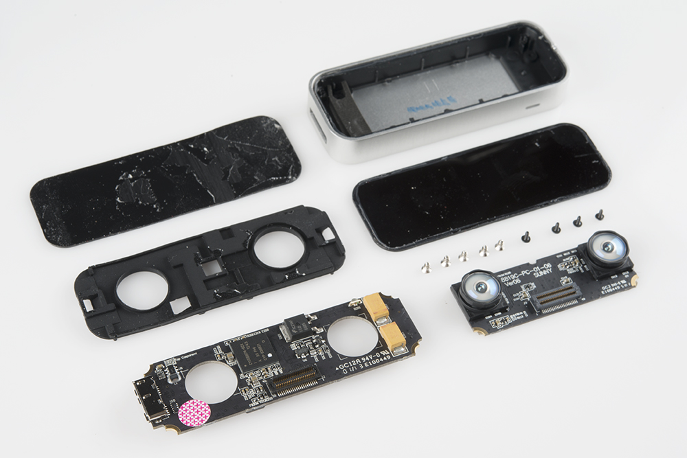
There you have it, folks--the Leap Motion in all its shattered glory. I plugged it in and tried it out while it was in pieces and it still works surprisingly well. That said, it works much better with the packaging in place.
I'm pretty impressed by the simplicity of it, but I can't say I'm all that surprised. As with the Google Glass Teardown, it's pretty clear that the magic is in the code, not the hardware. I'm also impressed by the thought that went into the design. Clearly, the Leap Motion folks have some skilled engineers putting some thought into how to make a durable, quality product.
Resources and Going Further
For more disassembling goodness, check out these other SparkFun teardowns:
- Nest Thermostat Teardown - Check out the original SFE Nest teardown.
- Nest Protect Teardown
- Google Glass Teardown (Sponsored by SFE)